ELECTRONIC COMPONENTS STORE
Explore, Create, and Innovate with Our Wide Range of Electronic Supplies
- Delivery is £1.90, Expected delivery time is 1-2 days, Free for orders over £25
- Fast Shipping from UK- Join Our Growing Community!
- Best Prices for Affordable Projects
- FNIRSI Oscilloscopes
- Soldering Iron Kits & Accessories
- Soldering Stations
- YIHUA
- On Sale
- Best Sellers
- Electronic Testing Equipment
- Accessories
- Audio Board Amplifiers
- Compatible with Arduino
- Wemos D1 Mini Boards – WiFi & Bluetooth
- Compatible with Arduino Starter Kits
- Arduino Sensors
- Communication Boards
- Arduino Shields
- Rechargeable Lithium Polymer Batteries
- Microcontroller Boards with WiFi & Bluetooth – ESP32, ESP8266
- Electronic Components
- DC to DC Converters – Buck, Boost & Buck-boost Converters
- Relay Modules
- Servo Motors and Motor Drivers
- Electronics Tools
- Uncategorized

Categories


Electronic Components on Sale
ESP32C3 Arduino Development Board WIFI Bluetooth5.0
Sale! Original price was: £9.90.£8.90Current price is: £8.90.Add to basket
Mini Raspberry Pi RP2040 -Zero (Compatible) Microcontroller Soldered/Unsoldered
Sale! Original price was: £8.90.£4.90Current price is: £4.90.Select options
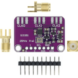
DC 3V-5V CJMCU-5351 Si5351A Si5351 I2C Clock Signal Generator Breakout Board
Sale! Original price was: £5.45.£4.45Current price is: £4.45.Add to basket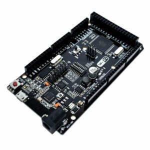
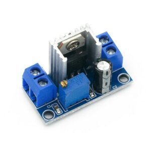
LM317 Buck Step Down Adjustable Voltage Converter
Sale! Original price was: £1.99.£1.45Current price is: £1.45.Add to basket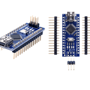
Arduino Nano V3.0 Compatible ATmega328P CH340 5V 16MHz
Sale! Original price was: £5.90.£4.90Current price is: £4.90.Select options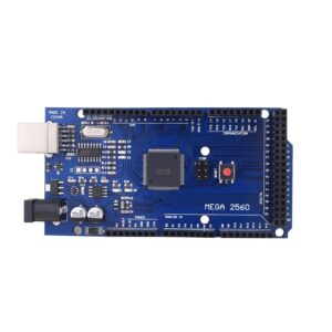
Arduino MEGA 2560 Compatible Development Board
Sale! Original price was: £17.90.£15.90Current price is: £15.90.Add to basket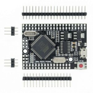
Arduino MEGA 2560 PRO Compatible
Sale! Original price was: £18.90.£13.90Current price is: £13.90.Add to basket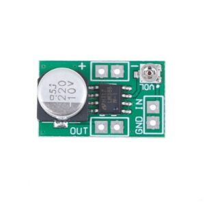
LM386 Mini Micro Audio Power Amplifier Board DC 3V~12V
Sale! Original price was: £3.90.£2.90Current price is: £2.90.Add to basket
Best Selling Components
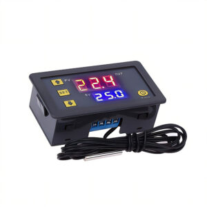
12V Temperature Controller Switch with Probe 20A Thermostat Control
Sale! Original price was: £6.90.£5.90Current price is: £5.90.Add to basket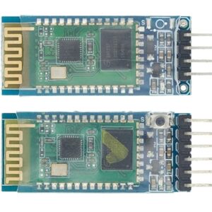
4Pin HC-05 HC-06 Bluetooth Wireless Serial Transceiver Module
Sale! Original price was: £4.90.£3.90Current price is: £3.90.Select options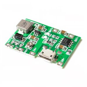
Battery Charger Board 18650 Lithium Li-ion 3.7V 4.2V DC-DC Step Up Boost Module TP4056
Sale! Original price was: £2.75.£2.45Current price is: £2.45.Add to basket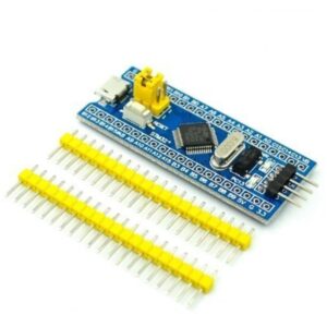
STM32F103C8T6 ARM STM32 -Blue Pill Dev Board (Clone Chip)
Sale! Original price was: £4.90.£2.90Current price is: £2.90.Add to basket
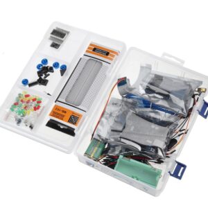
DIY Electronic Starter Kit Compatible with Arduino UNO
Sale! Original price was: £34.50.£27.90Current price is: £27.90.Add to basket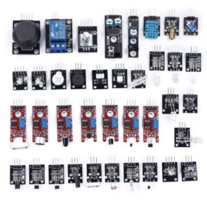
37pcs Sensor Kit for Arduino
Sale! Original price was: £15.90.£13.90Current price is: £13.90.Add to basket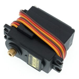
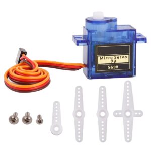
MG995 Servo Motor All Metal Gears For JR 2C RC 1/8 and 1/10 vehicles
Sale! Original price was: £4.90.£3.90Current price is: £3.90.Add to basketSame Day Shipping before 3 p.m.
30 Days Returns
FREE UK DELIVERY*
FNIRSI Products
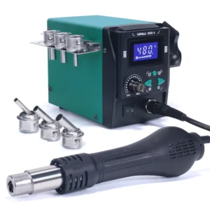
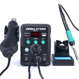
YIHUA 8786D 2 in 1 Hot Air Soldering and Rework Station
Sale! Original price was: £89.00.£79.00Current price is: £79.00.Add to basket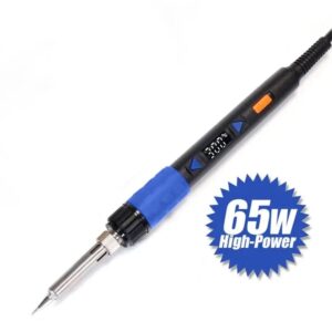
YIHUA 928d-I Soldering Iron 65W -UK Plug
Sale! Original price was: £22.90.£19.90Current price is: £19.90.Add to basket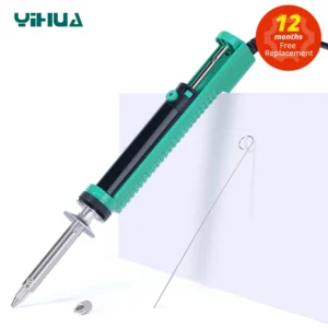
YIHUA 929D-V Electric Desoldering Pump Iron
Sale! Original price was: £17.90.£14.90Current price is: £14.90.Add to basket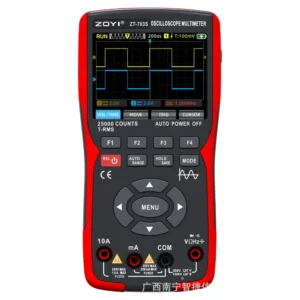
ZOYI ZT-703S 3 in 1 Handheld Digital Oscilloscope Multimeter
Sale! Original price was: £119.00.£99.00Current price is: £99.00.Add to basket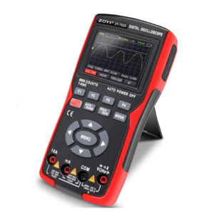
Zoyi ZT-702S Digital Oscilloscope Multimeter
Sale! Original price was: £69.00.£59.00Current price is: £59.00.Add to basket
ZOYI ZT102A Digital Multimeter
Sale! Original price was: £19.90.£18.90Current price is: £18.90.Add to basket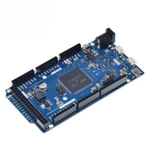

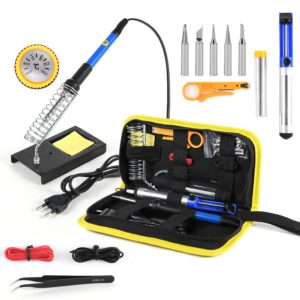
Basic Soldering Iron Kit UK Plug 60W
Sale! Original price was: £16.90.£14.90Current price is: £14.90.Add to basket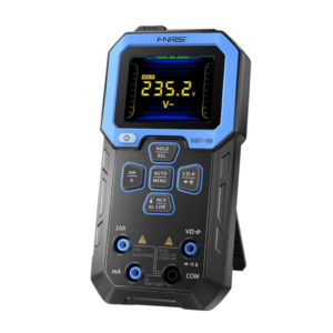
FNIRSI DMT-99 Digital Multimeter
Sale! Original price was: £49.90.£39.00Current price is: £39.00.Add to basket
Arduino Boards
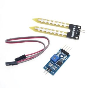
Soil Moisture Detection Sensor for Arduino
Sale! Original price was: £2.90.£1.90Current price is: £1.90.Add to basket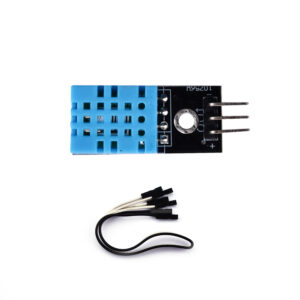
DHT11 Sensor Digital Temperature and Humidity Sensor
Sale! Original price was: £3.90.£3.45Current price is: £3.45.Add to basket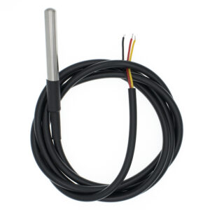
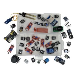
45pcs Sensor Kit for Arduino
Sale! Original price was: £29.90.£21.90Current price is: £21.90.Add to basket
AHT10 Digital Temperature and Humidity I2C
Sale! Original price was: £4.55.£3.45Current price is: £3.45.Add to basket
Welcome to Kunkune – Your Trusted UK Based Electronic Component Store
We are dedicated to providing DIY electronics enthusiasts, electronics hobbyists, and professionals with top-quality electronic components and Arduino kits.
Whether you’re a seasoned expert or just starting out, our extensive range of products ensures that you have everything you need to bring your electronic projects to life.
-Customer-Centric Approach: Our primary focus is you, our valued customer. We understand the importance of quality, affordability, and reliability.
That’s why we’ve been consistently providing easy-to-use Arduino Starter Kits, Arduino Sensors, Arduino boards, ESP32, ESP8266, Wemos D1 mini, Servo motors, and much more.
-Competitive Prices: At Kunkune we source the best products and offer them at unbeatable prices. Our goal is to make electronics accessible to everyone without breaking the bank.
-Fast Shipping: We understand the excitement of starting a new project and the importance of timely deliveries. That’s why we offer fast shipping options, including Standard 24H service and Next Day Special Delivery. With our partners from Royal Mail, you can be assured of receiving your products right on time.
-UK Based Operations: All our products are located in the United Kingdom, ensuring quick deliveries and easy returns. If you need larger quantities or specific items not in stock, rest assured, we can arrange it for you within 10 business days.
We invite you to explore our store and discover the endless possibilities that electronics offer. Whether you’re working on a school project, a personal hobby, or a professional assignment, Kunkune is here to support your journey. We hope our products inspire you to create, innovate, and achieve your electronic dreams.